Simple Configurable Logic Block on Tiny Tapeout
A 3 bit CLB on Sky130
Introduction
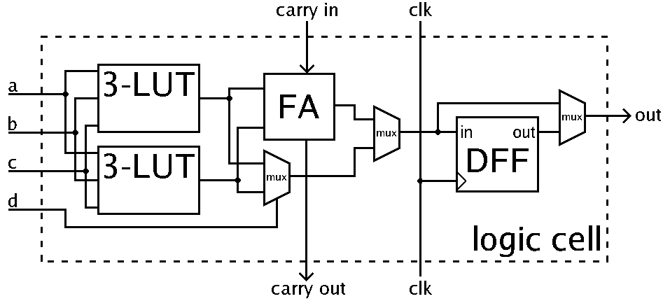
Field programmable gate arrays are integrated circuits designed to deploy digital circuits outside of the fab. The base of any FPGA architecture is the configurable logic block or CLB. At the base level a CLB contains a look-up table or LUT, a full adder, and flip flop. This Tiny Tapeout design implements a simple configurable logic block with a 3-bit look up table.

This document will detail a background of elements with a CLB, design choices taken in this IC’s design, verification flow and test structure, and results of this design flow.
Look Up Tables
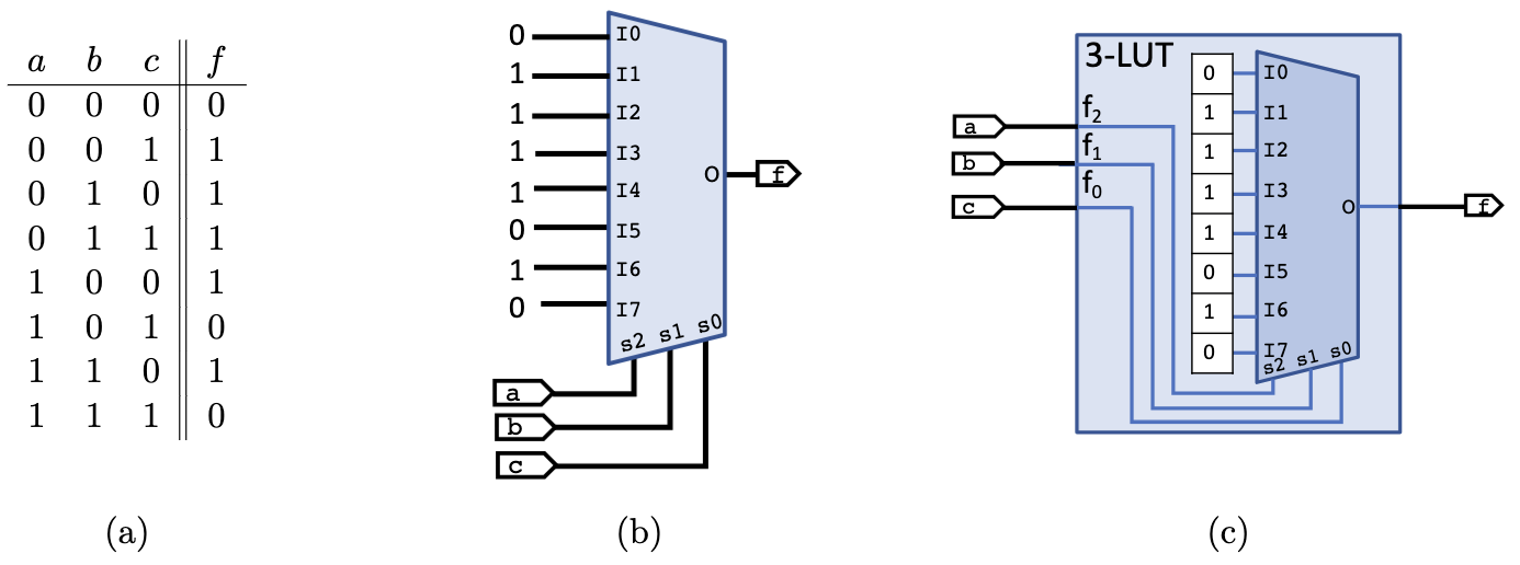
To allow universal boolean function support, a function is loaded into the LUT as a binary string. LUTs are memories connected to n to 1 muxes. The selector signals are used to “evaluate” the function and produce an output. LUT naming convention is LUTk, where k is the number of bits in the selector signal of the mux. Common LUT sizes are LUT4 and LUT6. A LUTk can represent of up to 2^(2^k) boolean functions. Below is an example of boolean function being loaded into a LUT and evaluated.

Flip Flops
For synchronous circuits, a flip flop is attached to the end of the CLB. A mux is provided and controlled by the synthesis tool to either send a the output of the LUT synchronous to the clock or by pass it and send it as a combinational output.
Full Adder
Since addition is a common arithmetic operation and a combinational function, a full adder is sometimes included inside a CLB. The carry logic is used to improve the efficiency of common arithmetic functions like addition, subtraction, counting, comparision, etc.
Tiny Tapeout Design
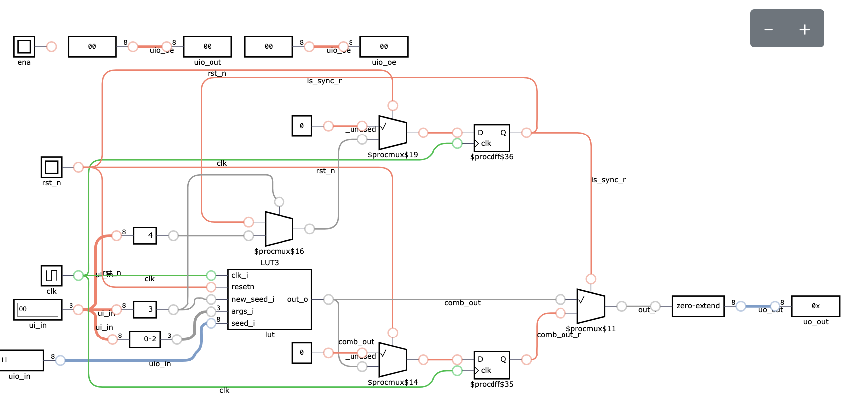
Due to the IO constraints of Tiny Tapeout, several design choices had to be made. For one, no full add logic is included in this design. While there is space on the IO pads for a full adder enable and output, there is no space for another CLB to showcase the carry out for arithmetic efficiency. Additionally a LUT3 is used since there are 8 bits dedicated to input and bi-directional ports. Meaning the entire bi-directional bus is used for inputting a boolean function and the dedicated input ports are entirely for control. This means there is only 1 bit dedicated to output and supports all 256 ternary boolean functions. Below is the logical schematic synthesized by Yosys and rendered by DigitalJS.

LUT3 Design
As mentioned before, due to IO constraints a LUT3 is implemented. There are two main choices in implementing the memory for the LUT: SRAM or flip flops. Flip flops are simple to implement in RTL as it is just the synthesizers job but have 8 extra nets added to the clock net. SRAMs only have a single connection to the clock net for write enable and are smaller, but require an external memory compiler, changes to the config file, and there are not enough bits to remember to justify them. Additionally, given that the design already is small enough, the extra routing and clock tree synthesis for 8 flip flops is not that big of a deal.
The IO for this module is simple and works as follows:
| Port | Direction | Width | Description |
|---|---|---|---|
| clk_i | Input | 1 | Clock for FFs |
| resetn | Input | 1 | Active low reset for FFs |
| new_seed_i | Input | 1 | Clock enable for FFs to take in a new seed/function |
| args_i | Input | 3 | Arguments in the function to evaluate it |
| seed_i | Input | 8 | Represents boolean function to be held in FFs |
| out_o | Output | 1 | Evaluation of the function given arg_i |
Below is a waveform of loading in NAND3 functionality into the LUT.

Once the new_seed_i signal is high is the new function stored in the LUT. Since we have programmed a NAND3, we only see out_o go low when all 3 arguments are high.
Top Module
Given that the full adder and carry logic are omitted from this IC due to IO constraints, the top module is just describing the multiplexing of the LUT3’s direct output and the output of a flip flop driven by the LUT3. This is done by saving the ui_in[4] input in a separate flip flop when ui_in[3] is high to send in a new seed in the LUT3. When ui_in[4] is high, the final output is driven by the flip flop rather than directly by the LUT3.
Below is a description of the IO for the top module.
| Port | Direction | Width | Description |
|---|---|---|---|
| clk | Input | 1 | Clock for the entire design, at 50Mhz |
| rst_n | Input | 1 | Active low reset for entire design |
| ui_in | Input | 8 | Dedicated Input |
| uio_in | Input | 8 | Input path of the bi-direction IO, dedicated entirely to the seed/function |
| ena | Input | 1 | Used by Tiny Tapeout, ignored |
| uo_out | Output | 8 | Dedicated Output |
| uio_out | Output | 8 | Output path of the bi-directional IO, unused |
| uio_oe | Output | 8 | Enable path of the bi-directional IO, set low to only use input path |
Below is a description of the ui_in bus separated by bits.
| Port | Direction | Width | Description |
|---|---|---|---|
| ui_in[0] | Input | 1 | Input C of the boolean function, also the LSB of the function |
| ui_in[1] | Input | 1 | Input B of the boolean function |
| ui_in[2] | Input | 1 | Input A of the boolean function, also the MSB of the function |
| ui_in[3] | Input | 1 | When high writes in what uio_in holds in the LUT3 FFs and saves synchronous setting |
| ui_in[4] | Input | 1 | Selects the between outputting the direct LUT3 output or from a FF, saved when ui_in[3] is high |
| ui_in[7:5] | Input | 3 | Unused |
Below is a description of the uo_out bus separated by bits.
| Port | Direction | Width | Description |
|---|---|---|---|
| uo_out[0] | Output | 1 | Evaluation of the boolean function given the args, synchronous depending on the state of ui_in[4] |
| uo_out[7:1] | Output | 7 | Unused |
Common Functions
Here is a table for common 3 bit boolean functions and the corresponding seed to program the CLB.
| Function | Seed/uio_in[7:0] |
|---|---|
| NAND3 | 01111111 |
| NOR3 | 00000001 |
| NOT | 01010101 |
| XOR2 | 01100110 |
| Majority | 11101000 |
| Even Parity | 01101001 |
| One Hot | 00010110 |
Verification
Given the RTL itself is simple and did not take a lot of time, most of the effort went into verification. Since Tiny Tapeout is aimed at those with little to no hardware design experience, it uses coco-tb, a Python framework, for the test flow. A vcd (value change dump) file is produced to create a waveform that is displayed in a waveform viewer of choice. During this project, a Github Codespaces was used to facilitate development over the web without any local installation of any tool and used the default waveform viewer provided: Surfer.
Test Design
Extensive effort was spent optimizing tests. There is a main test that simply calls all other test functions. This main test thread holds a dictionary mapping strings to boolean integer literals as shown below.
seeds = {"not": 0b01010101, "and2": 0b10001000, "or2": 0b11101110, "xor2": 0b01100110,
            "nand2": 0b01110111, "nor2": 0b00010001, "nand3": 0b01111111,
            "nor3": 0b00000001,"majority": 0b11101000, "even_parity": 0b01101001,
            "one_hot":0b00010110}
Each test function is an async Python or co-routine that takes in 3 arguments: a “dut” argument which is the main top module as a Python class, “seed” which is an integer representing the function to be programmed and tested in the CLB, “sync” a boolean defaulted to false representing if the flip flop attached to the end of the CLB is used or bypassed. Note, binary boolean functions treat the MSB of the arg_i input as a don’t care signal for this testbench. Below is the co-routine to test the NAND3 function.
async def test_a_b_c_nand(dut,seed,sync=False):
    dut._log.info(f"Start Test: A nand B nand C | Is Sync:{sync}")
    dut.uio_in.value = seed
    sync_mask = int(sync) << 4
    sync_cycles = 2 if sync else 1
    dut.ui_in.value = 0b00001000 | sync_mask
    await ClockCycles(dut.clk,1)
    dut.ui_in.value = 0b00000000 | sync_mask
    await ClockCycles(dut.clk,1)
    input_value = 0
    while(input_value != 8):
        dut.ui_in.value = input_value | sync_mask
        a_value = input_value & 0b00000001
        b_value = (input_value & 0b00000010) >> 1
        c_value = (input_value & 0b00000100) >> 2
        await ClockCycles(dut.clk,sync_cycles)
        dut._log.info(
            f"
            A:{bin(a_value)} B:{bin(b_value)} C:{bin(c_value)} Out:{dut.uut.uo_out.value}
            ")
        assert dut.uo_out.value == (~(a_value & b_value & c_value) & 0b00000001)
        input_value += 1
    await ClockCycles(dut.clk,1)
Co-routines begin with logging the function to be tested. To handle synchronous selection a sync mask is created and bitwise OR’ed with inputs into ui_in assignments. This works since synchronous selection is an active high signal. When the CLB flip flop is used a 2 cycle wait is used and 1 if it bypassed since the testbench moves the clock by cycles rather than edges. First the seed is loaded and CLB bypassed is selected. After this sequence a while loop is ran. An assert is ran checking the value of the CLB compared to a Python evaluation of the function after an appropriate amount of cycles is passed. The loop terminates after the number 8 is reached since this means we have checked all possible arguments into the function.
Waveforms
A total of 11 boolean functions are tested. Each function is tested for asynchronous and synchronous output for a total of 22 waveforms to analyze. For brevity of this report, we will analyze both the even-parity and majority functions.
Even Parity
The function for even parity is as follows:
\[f(a,b,c) = \lnot (a \oplus b \oplus c)\]For the function to be satisfied, there must an even amount of 1’s in the argument bus. The waveform below shows the asynchronous behavior of the even parity function.

It is shown here that when ui_in[2:0] has an even amount of 1’s, the unit under test outputs a 1. This output happens immediately after a new input into ui_in[2:0]. Below is the synchronous behavior of the even parity function.

When ui_in[4] is asserted high and a new seed is loaded, the unit under test only outputs the function’s evaluation a cycle later on the positive edge of the clock. We still get the same evaluation per input just with the one cycle delay.
Majority
The function for even parity is as follows:
\[f(a,b,c) = a \land b \land \lnot c \lor a \land \lnot b \land c \lor \lnot a \land b \land c \lor a \land b \land c\]For the function to be satisfied, there must a majority amount of 1’s out of 3 in the argument bus. The waveform below shows the asynchronous behavior of the majority function.

It is shown here that when ui_in[2:0] has 2 or 3 1’s, the unit under test outputs a 1. This output happens immediately after a new input into ui_in[2:0] as expected. Below is the synchronous behavior of the majority function.

Other Waveforms
The final testbench dumps all 22 tests onto one vcd file. They are ordered in as written by this code body of the main test function:
    await test_a_not(dut,seeds["not"])
    await test_a_b_and(dut,seeds["and2"])
    await test_a_b_or(dut,seeds["or2"])
    await test_a_b_xor(dut,seeds["xor2"])
    await test_a_b_nand(dut,seeds["nand2"])
    await test_a_b_nor(dut, seeds["nor2"])
    await test_a_b_c_nand(dut,seeds["nand3"])
    await test_a_b_c_nor(dut,seeds["nor3"])
    await test_a_b_c_majority(dut,seeds["majority"])
    await test_a_b_c_even_parity(dut,seeds["even_parity"])
    await test_a_b_c_one_hot(dut,seeds["one_hot"])
    await test_a_not(dut,seeds["not"],True)
    await test_a_b_and(dut,seeds["and2"],True)
    await test_a_b_or(dut,seeds["or2"],True)
    await test_a_b_xor(dut,seeds["xor2"],True)
    await test_a_b_nand(dut,seeds["nand2"],True)
    await test_a_b_nor(dut, seeds["nor2"],True)
    await test_a_b_c_nand(dut,seeds["nand3"],True)
    await test_a_b_c_nor(dut,seeds["nor3"],True)
    await test_a_b_c_majority(dut,seeds["majority"],True)
    await test_a_b_c_even_parity(dut,seeds["even_parity"],True)
    await test_a_b_c_one_hot(dut,seeds["one_hot"],True)
To view all tests follow the steps below.
- Click to download the final vcd file: tb.vcd
- Go to Surfer Waveform Viewer on your browser of choice
- Go to File -> Open file -> Browse -> Path to tb.vcd
- Click on tb under the Scope tab and add in the following signals: clk,rst_n, ui_in, uio_in, uo_out
- Right on ui_in, uio_in, uo_out, Format -> Binary
- Click on “Zoom to fit”
- Scroll left to see behavior
Results
The final design is a result of the Openlane flow to produce a GDSII file for the fabrication process. This section reports area usage, cell usage, and routing statistics.
CLB Area Usage

| Utilisation (%) | Wire length (um) |
|---|---|
| 3.600 % | 1058 |
This makes sense as this design conceptually is just an 8-bit register attached to a 8 to 1 multiplexor with a flip flop. Above is the schematic viewer produced by the GDS Github Actions job to produce the GDSII file.
CLB Cell Usage
| Category | Cells | Count |
|---|---|---|
| Fill | decap fill | 1443 |
| Tap | tapvpwrvgnd | 225 |
| Misc | conb dlygate4sd3 | 27 |
| Buffer | clkbuf buf | 19 |
| Multiplexer | mux2 mux4 | 11 |
| Flip Flops | dfxtp | 10 |
| AND | and2 | 9 |
| Combo Logic | and2b a21bo o221a o31a o21a | 6 |
| NAND | nand2b | 1 |
This breakdown of cells used again makes sense due to the simplicity of the final design. A total of 83 cells excluding tap and fill cells are used. An interesting item of note is the flip flop cell count. 10 flip-flops are easily spotted inside the RTL. Within the LUT3.v there the following code block:
  reg [7:0] lookup_table_r;
  reg out_r;
  always @(posedge clk_i) begin
    if(!resetn) begin
      lookup_table_r <= '0;
    end
    else if (new_seed_i) begin
      lookup_table_r <= seed_i;
    end
  end
Here is an 8 bit bus called “lookup_table_r” that is driven by a synchronous block. Openlane sees this to create an 8-bit flip flop register, thus this Verilog module is responsible for 8 out of the 10 flip flops. The other 2 are found in the top module in the following code block:
  always @(posedge clk) begin
    if(!rst_n) begin
      is_sync_r <= 1'b0;
    end else if(ui_in[3]) begin
      is_sync_r <= ui_in[4];
    end
  end

  //ff for a sync clk - will be a 2 cycle delay with this LUT design
  always @(posedge clk) begin
    if(!rst_n) begin
      comb_out_r <= '0;
    end else begin
      comb_out_r <= comb_out;
    end
  end
These two synchronous blocks create the other 2 flip flops. Just by reading the RTL itself we as humans can extrapolate a total of 10 flip-flops used in this entire design.
NAND3 Comparison
A question to be asked is how do dedicated ASICs compare final CLB. To benchmark the CLB against a NAND3 design was submitted to a seperate branch for GDS Github Action workflows. Below are area usage percentage and usage by cell for the NAND3 design.
| Utilisation (%) | Wire length (um) |
|---|---|
| 0.605 % | 169 |
| Category | Cells | Count |
|---|---|---|
| Fill | decap fill | 1471 |
| Tap | tapvpwrvgnd | 225 |
| Misc | conb | 23 |
| Buffer | buf | 3 |
| NAND | nand3 | 1 |
As expected only a single NAND3 cell is used here, along with miscellaneous cells. By itself NAND3 uses 0.605% of the die with only 169 microns for wire length. Compared to the CLB this is a 6x area improvement and 6.3x wiring improvement. Less wiring means less delay in data movement and possibly mean a faster clock for the ASIC design than the CLB. Area improvement means the die can be used for other logic or macros. However this design can only do a NAND3 function, anything else is moot. Our CLB can represent 255 other 3-bit boolean functions as well as control wether that function is outputted synchronously to a clock edge. However this does come at area and performance penalties. This showcases clearly the pros and cons to an ASIC design compared to an FPGA design. The designer must make the decision of if the circuit requires the performance and mass scale production to deploy it on a custom ASIC, and receive it months later. Or the designer may choose to deploy their circuit in the field at the cost of performance.
Conclusion
Despite the simplicity of this project, it was entertaining putting it all together. 256 total boolean functions is a deceptively bigger number of functions 3-bits can load. Additionally this project teaches one the trade offs that come with the decision of choosing between an ASIC or FPGA for a project. Most VLSI courses mention the area and performance penalties of FPGAs compared to a custom ASIC yet never show why. Here it is shown why. Testing too was more entertaining that anticipated. Given the simplicity of the project, it is simple to modularize a test structure. Especially with cocotb, one can utilize Python data structures to make readable tests.
References
Look Up Table image is taken from: Schlag, M. (2024). Beginning Logic Design. Retrieved from https://escholarship.org/uc/item/9q1786xf